
How to Choose the Right Depth Profiling Method for Your Materials
Why Choosing the Right Method for Depth Profiling Elements Changes Everything
When it comes to depth profiling elements in real materials, the method you choose can mean the difference between actionable data and an expensive dead end. Different techniques vary wildly in depth resolution, sensitivity, which elements they can detect, and whether they destroy your sample in the process.
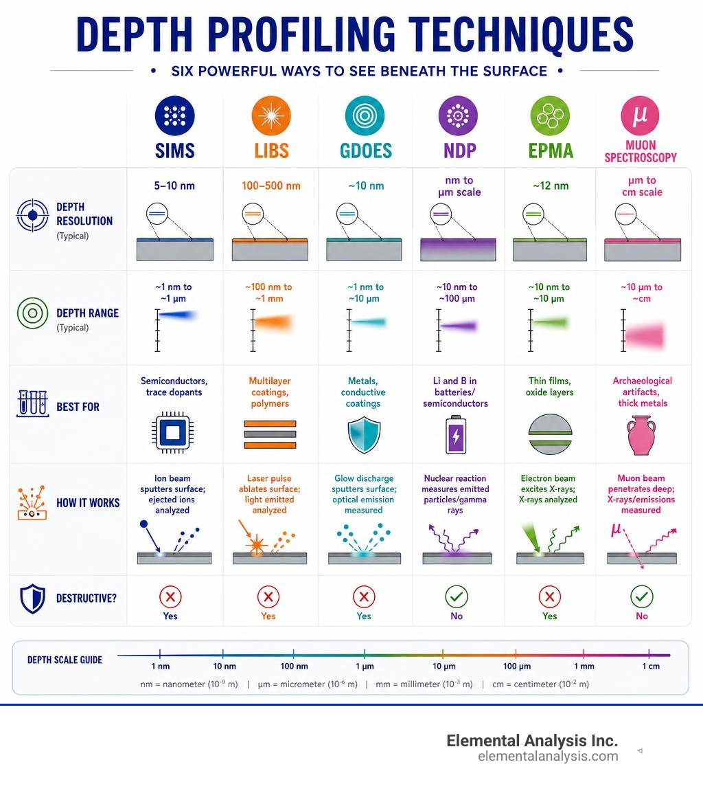
Here is a quick-reference guide to the most common depth profiling methods:
| Technique | Depth Resolution | Destructive? | Best For |
|---|---|---|---|
| SIMS | 5–10 nm | Yes | Semiconductors, trace dopants |
| LIBS | 100–500 nm | Yes | Multilayer coatings, polymers |
| GDOES | ~10 nm | Yes | Metals, conductive coatings |
| EPMA-SDP | ~12 nm | Yes | Thin films, oxide layers |
| NDP | nm to µm scale | No | Li and B in batteries/semiconductors |
| Muon spectroscopy (µ-XES) | µm to cm scale | No | Archaeological artifacts, thick metals |
| PIXE/XRF | µm scale | No | Surface and near-surface bulk analysis |
The stakes are high. Consider this: SIMS can detect a trace element at just 20 parts per billion within a sample volume of one ten-billionth of a cubic centimeter. That level of sensitivity is remarkable — but it is completely useless if you pick the wrong technique for your matrix, your budget, or your required depth range.
The right method depends on your material, your target elements, your depth range, and whether you can afford to consume the sample.
This guide walks you through the physics behind each major technique, how they compare on performance, and which real-world scenarios call for which approach — so you can make a confident, informed decision before committing samples or budget.
Essential depth profiling elements terms:
Fundamental Principles of Depth Profiling Elements
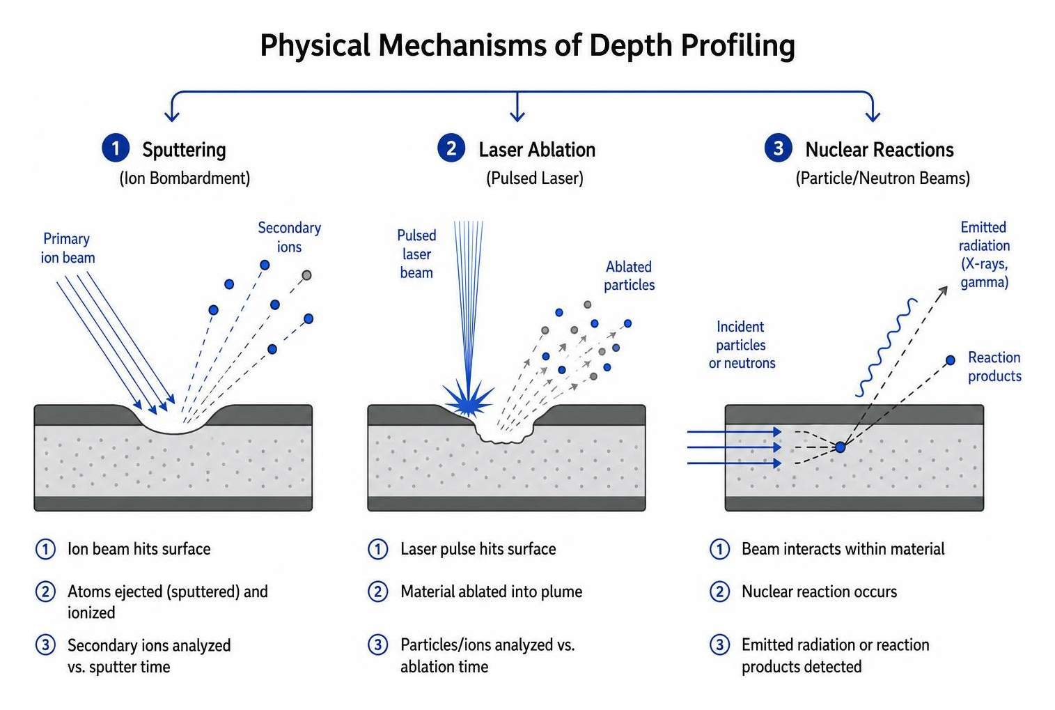
To successfully measure how elements are distributed beneath a surface, we must first understand the physical mechanisms used to uncover them. Broadly speaking, depth profiling techniques rely on one of two strategies: either physically eroding the sample layer-by-layer to analyze the released material, or using highly penetrating beams of light, neutrons, or subatomic particles to probe deep into the matrix non-destructively.
Secondary Ion Mass Spectrometry (SIMS) for Depth Profiling Elements
Secondary Ion Mass Spectrometry (SIMS) is the gold standard for high-sensitivity depth profiling. The fundamental mechanism relies on ion bombardment. We focus a primary ion beam (typically keV-energy ions such as cesium, oxygen, or argon) onto the sample surface. This beam initiates a collision cascade, physically sputtering away the outermost atomic monolayers.
As these surface atoms are ejected, a small fraction of them are ionized. These “secondary ions” are accelerated into a mass spectrometer, which filters and counts them based on their mass-to-charge ratio. By continuously monitoring these secondary ion signals over time as the primary beam drills a crater into the sample, we obtain a raw profile of signal intensity versus sputtering time.
Conventional keV SIMS excels at extreme surface sensitivity, but it is notorious for matrix effects—where the ionization efficiency of an element changes dramatically depending on the surrounding chemical environment. Recent advances, such as those detailed in the study on the depth profiling of Cr-ITO dual-layer sample with secondary ion mass spectrometry using MeV ions in the low energy region | Scientific Reports, show that utilizing Low Energy (LE) MeV SIMS (such as a 555 keV copper ion beam) can dramatically suppress these artificial intensity spikes at oxidized thin-film interfaces, offering a clearer picture of the true elemental boundaries. For a deeper understanding of achieving trace detection limits in mass spectrometry, see our In-Depth Guide to Low Detection Limits.
Laser-Induced Breakdown Spectroscopy (LIBS) and Glow Discharge (GDOES)
When we need to profile deeper coatings or multilayer materials at faster speeds, we often turn to laser ablation or cathodic sputtering.
Laser-Induced Breakdown Spectroscopy (LIBS) performs depth profiling by focusing high-energy laser pulses onto a sample. Each pulse ablates a microscopic amount of material, typically stripping away a layer between 100 and 500 nm thick. This process generates a highly excited plasma plume. As the atoms and ions within this plasma cool, they emit characteristic light. By capturing this emission spectra pulse-by-pulse, we can map the elemental composition as a function of depth.
The dynamics of this process are highly complex; as explored in the academic review on the Application of Laser-Induced Breakdown Spectroscopy for Depth Profiling of Multilayer and Graded Materials – PMC, controlling crater geometry and laser fluence is absolutely critical to preventing redeposition and maintaining depth resolution. To understand how laser ablation couples with other mass spectrometry techniques, read our article on What is Laser Ablation ICP-MS and How Does It Work?.
Glow Discharge Optical Emission Spectroscopy (GDOES), on the other hand, relies on cathodic sputtering within a low-pressure noble gas plasma (usually argon or neon). The sample itself acts as the cathode in a Grimm-type spectral source. Under a high voltage (typically -700 to -1200 V), gas ions accelerate toward the sample surface, eroding it uniformly. The sputtered atoms are then excited in the plasma glow discharge, emitting characteristic light.
As outlined in the comprehensive review on Depth-Resolved Elemental Analysis by Glow Discharge Emission Spectroscopy: Practical Aspects—A Review, GDOES can operate in either Direct Current (DC) mode for conductive materials or Radio Frequency (RF) mode, which uses capacitive coupling to develop a negative bias on non-conductive samples like ceramics or thick glass.
Neutron Depth Profiling (NDP) and Electron Probe Microanalysis (EPMA)
For non-destructive or highly quantitative submicron profiling, we look to nuclear reactions and electron-beam interactions.
Neutron Depth Profiling (NDP) is a completely non-destructive technique that relies on neutron-induced nuclear reactions. When a thermal neutron beam (typically less than 30 mm in diameter) strikes a sample, specific isotopes (like helium-3, lithium-6, or boron-10) capture a neutron and immediately decay, emitting energetic charged particles (protons or alpha particles). As these charged particles travel through the sample host matrix toward the detector, they lose energy in a highly predictable, depth-dependent manner. By measuring the residual energy of the escaping particles, we can calculate the exact depth from which they originated. This makes NDP an invaluable tool for battery and semiconductor research. To see how this fits into the broader landscape of neutron-based testing, check out A Comprehensive Guide to Neutron Activation Analysis.
Electron Probe Microanalysis (EPMA), combined with Wavelength Dispersive Spectroscopy (WDS), is traditionally a bulk analysis tool. However, by combining it with physical ion sputtering—a technique known as EPMA Sputter Depth Profiling (EPMA-SDP)—we can achieve quantitative submicron depth profiles. The primary electron beam excites characteristic X-rays within a small excitation volume.
As detailed in the pioneering paper EPMA Sputter Depth Profiling: A New Technique for Quantitative, by systematically sputtering the sample and taking microprobe measurements along the crater edge, we can reconstruct the original depth profile with exceptional quantitative accuracy.
Comparing Analytical Performance Across Techniques
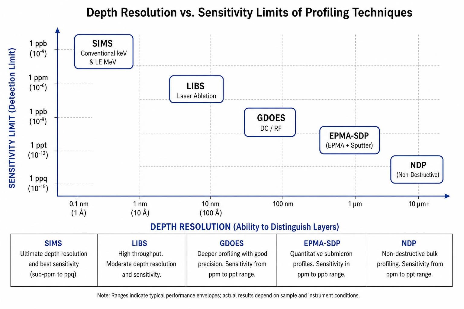
Choosing the right technique requires balancing several competing performance metrics. No single method is perfect for every scenario; some sacrifice depth resolution for extreme sensitivity, while others trade trace detection limits for non-destructive bulk mapping.
Depth Resolution and Sensitivity Limits
When analyzing advanced nanostructures, depth resolution—the ability to distinguish between two closely spaced layers—is paramount. SIMS is the undisputed leader here, routinely achieving a depth resolution in the 50–100 Å (5–10 nm) range, even at depths exceeding 10,000 Å.
In terms of sensitivity, SIMS can detect virtually all elements from hydrogen to uranium with sub-part-per-million (ppm) sensitivity. To put this in perspective, in a gallium arsenide (GaAs) sample ion-implanted with silicon, SIMS successfully detected a peak concentration of only 10 parts per million atomic (ppma) down to a background level of 20 parts per billion atomic (ppba). The physical volume analyzed per data point was a minuscule 1E-10 cc, containing only about 100,000 atoms (2E-19 moles) of silicon.
LIBS, by contrast, operates on a much larger scale. Its typical depth resolution falls between 100 and 500 nm, making it less suitable for thin-film interfaces but excellent for thick, graded coatings. However, LIBS is highly sensitive to almost the entire periodic table, with detection limits for many elements in the 1–100 µg/g range. For those working with nanometer-scale materials where traditional profiling might destroy delicate features, our guide on How to Characterize Nanomaterials Without Losing Your Mind offers alternative strategies.
Detectable Elements and Quantitative Accuracy
The capability to detect light elements is a major dividing line among these techniques. Standard energy-dispersive XRF and Particle-Induced X-ray Emission struggle with very light elements (Z < 11). GDOES, LIBS, and SIMS, however, easily detect light elements like hydrogen, lithium, beryllium, boron, and carbon.
When it comes to quantitative accuracy, raw data can be highly misleading due to matrix effects. However, when properly calibrated with ion-implanted standards, SIMS can routinely measure elemental concentrations to within 10–20% accuracy, with better than 5% possible under ideal conditions.
EPMA-SDP also shines in quantitative accuracy, achieving a relative accuracy of 10% for elemental composition variations with depth. It can detect incredibly small elemental coverages down to 10^14 atoms per cm² if the element is not already present in the substrate.
Overcoming Calibration and Physical Challenges in Depth Profiling
The raw data generated by depth profiling instruments—usually measured as signal intensity versus sputtering time or laser pulse count—cannot be used directly for engineering decisions. Converting these raw signals into accurate concentration-versus-depth scales is one of the greatest challenges in analytical chemistry.
Converting Sputter Time and Laser Pulses to Depth Scales
Sputtering rates are rarely constant. They change as the beam penetrates different material layers, meaning a simple linear conversion of time-to-depth is often highly inaccurate.
To calibrate the depth scale, we typically use post-analysis physical measurements. After the profiling run is complete, we use a mechanical stylus profilometer, optical interferometry, or atomic force microscopy (AFM) to measure the exact physical depth of the sputtered crater. By dividing this final depth by the total sputtering time, we establish an average sputtering rate.
For complex multilayer systems, we must utilize advanced mathematical modeling. As discussed in EPMA Sputter Depth Profiling, Part I: Theory and Evaluation, researchers use Monte Carlo simulations and maximum entropy reconstruction algorithms to deconvolve the raw intensity profiles, separating the physical depth coordinate from the instrumental broadening caused by the excitation volume.
Managing Matrix Effects and Crater Morphology
Two physical phenomena constantly threaten the reliability of depth profiles: matrix effects and crater morphology.
The matrix effect is a phenomenon where the surrounding chemical environment alters the emission or ionization efficiency of a target element. In SIMS, for example, the presence of oxygen at an interface can artificially boost the secondary ion yield of metals by orders of magnitude, creating a false “spike” in concentration. We can manage this by using matrix-matched calibration standards or by transitioning to alternative techniques like GDOES, which uses relative “sputter factors” to normalize emission yields across different matrices. To learn more about standard elemental analysis and calibration, explore our guide on ICP technology.
Crater morphology is equally critical. To achieve high depth resolution, the bottom of the sputtered or ablated crater must remain perfectly flat. If the crater bottom is curved, or if the edges of the crater slope gradually, signal from the surface layers will mix with signal from the deeper layers, destroying the interface resolution. This is known as the crater edge effect. We mitigate this by:
- Rastering the primary ion or laser beam over a wide area and electronically gating the detector to collect signals only from the flat center of the crater.
- Maintaining a highly uniform laser beam profile (such as a flat-top beam) during LIBS depth profiling to prevent uneven “drilling.”
- Using low sputtering energies and rotating the sample during analysis to minimize sputtering-induced surface roughness.
Future Directions and Emerging Technologies in Depth Profiling
The boundaries of depth profiling are constantly expanding. One of the most exciting developments is Low Energy (LE) MeV SIMS. By utilizing heavy, high-energy primary ions in the hundreds of keV range, accelerator laboratories can now achieve deep profiling of inorganic thin films with minimal matrix effects and high interface resolution.
In Neutron Depth Profiling, the integration of multi-detector arrays (such as eight silicon detectors mounted in a ring format inside a vacuum chamber) has drastically increased count rates. This allows smaller, university-scale reactor facilities to achieve analytical efficiencies that were once only possible at massive national laboratories.
Furthermore, the application of advanced maximum entropy algorithms is allowing scientists to quantitatively reconstruct three-dimensional elemental distributions from noisy, raw depth-profiling data, opening up new frontiers in 3D materials characterization.
Real-World Applications for Depth Profiling Elements
Understanding the theory is only half the battle; knowing which technique to apply to a specific material class is what solves real-world engineering and research problems.

Semiconductor and Thin-Film Characterization
In the semiconductor industry, precise control over dopant profiles and junction depths is the key to device performance. SIMS is the undisputed choice for determining the total retained dose of ion-implanted species (such as boron, phosphorus, or arsenic) after thermal processing.
A major challenge in single-crystal semiconductors is the “ion channeling” effect, where implanted ions find open channels between rows of atoms and penetrate much deeper than standard amorphous models predict. To accurately profile these distributions, we must use SIMS calibrated with ion-implantation standards, which are exceptionally accurate because the dopant dose is known to within 1–2% in virtually any matrix.
Additionally, when traditional Fourier Transform Infrared (FTIR) spectroscopy fails to measure oxygen concentrations in highly doped silicon wafers (such as those used for latch-up resistant CMOS circuits), SIMS depth profiling provides the necessary sensitivity and spatial resolution. To understand how mass spectrometry handles these ultra-precise measurements, read ICP-MS Explained: How We Weigh Atoms in a Plasma Fire.
Non-Destructive Depth Profiling Elements in Heritage Science and Biology
While destructive techniques are perfect for industrial quality control, they are entirely unsuited for rare cultural heritage artifacts or delicate biological samples.
For these precious materials, we look to highly penetrating, non-destructive particles. Standard PIXE and XRF can map surface elements, but they are limited by self-absorption—where low-energy characteristic X-rays are absorbed by the sample itself before reaching the detector.
To bypass this limit, scientists are now utilizing negative muons. As detailed in Depth profiling the elemental composition with negative muons: Monte Carlo based tools for improved data analysis – ScienceDirect, negative muons are approximately 207 times heavier than electrons. When captured by an atom, they emit muonic X-rays with energies up to the MeV scale—energies so high they easily escape from deep within the sample without self-absorption.
This allows researchers to non-destructively profile the thickness of gold plating or identify corrosion patinas up to a full centimeter deep inside ancient bronze or silver artifacts. For complementary geological and archaeological testing, we also utilize specialized methods like PIXE and Unlocking Geological Secrets with Isotope Ratio ICP-MS.
Frequently Asked Questions about Depth Profiling
How do matrix effects impact depth profiling accuracy?
Matrix effects alter the ionization or emission efficiency of an element based on its surrounding chemical environment, rather than its actual concentration. For example, in SIMS, transition metals show a massive secondary ion yield enhancement when oxygen is present. If left uncorrected, this can lead to artificial concentration spikes at oxidized interfaces. To overcome this, we must use matrix-matched calibration standards or transition to techniques like GDOES or LE MeV SIMS, which are significantly less sensitive to chemical matrix variations.
What is the difference between destructive and non-destructive depth profiling?
Destructive depth profiling (such as SIMS, LIBS, and GDOES) physically erodes the sample layer-by-layer using ion sputtering or laser ablation to analyze the ejected material. This provides exceptional depth resolution and sensitivity but permanently consumes the sample. Non-destructive depth profiling (such as NDP, Muon Spectroscopy, or PIXE) uses highly penetrating incident beams to excite reactions deep within the material, measuring the energy loss of escaping particles or high-energy X-rays to calculate depth without altering the sample structure.
How is depth resolution defined and measured?
Depth resolution is quantitatively defined as the sputtered depth interval corresponding to the change in signal intensity from 84% to 16% of its maximum value at an ideally sharp, step-like interface. It represents the minimum distance required to distinguish two distinct elemental layers. Factors that degrade depth resolution include sputtering-induced surface roughness, crater bottom curvature (crater edge effects), and atomic mixing caused by high-energy primary ion bombardment.
Conclusion
Choosing the right method for depth profiling elements is not a one-size-fits-all decision. It requires a careful evaluation of your sample’s physical properties, your target depth range, required detection limits, and whether the sample must remain intact after analysis.
Whether you need the extreme, sub-parts-per-million sensitivity of SIMS for semiconductor dopants, the rapid multilayer profiling of GDOES and LIBS for industrial coatings, or the completely non-destructive precision of PIXE and neutron-based techniques, selecting the correct analytical pathway is what ensures the integrity of your data.
At Elemental Analysis Inc., we specialize in helping you navigate these complex analytical challenges. As the first commercial PIXE laboratory, we offer a comprehensive suite of destructive and non-destructive testing options designed to deliver fast, highly accurate, and competitively priced elemental identification and depth profiling solutions.
Ready to unlock the elemental secrets hidden beneath your material’s surface? Explore our full range of professional testing services and find the perfect analytical match for your project on our Elemental Analysis Services page.