
Mapping the Microscopic World with Elemental Mapping Analysis
Fundamentals of Chemical Distribution in Materials Analysis
When we look at a material under a standard microscope, we see surface texture, boundaries, and physical structures, but we cannot see what the sample is made of at every specific point. Elemental mapping analysis bridges this gap by combining spatial imaging with spectroscopic analysis. To understand how this works across different materials, exploring A Quick Start Guide to Elemental Analysis Methods offers a great foundation.
Instead of taking a single measurement across an entire sample, mapping divides a two-dimensional area into a grid of tiny points or pixels. At each pixel, the analytical instrument measures signals that are unique to specific chemical elements.
Principles of Spatial Energy Signal Acquisition
The fundamental principle behind most mapping systems relies on rastering a focused beam across a sample surface. In electron microscopy, an electron beam hits the specimen, knocking inner-shell electrons out of the atoms. As outer-shell electrons drop down to fill these vacancies, they emit characteristic X-rays.
Because each element has a unique atomic energy structure, these X-rays serve as chemical fingerprints. By detecting these emitted X-rays pixel-by-pixel, the system builds a 2D map of elemental distribution. However, analysts must keep matrix effects in mind. The depth to which the beam penetrates and the absorption of X-rays by neighboring atoms can influence signal strength, meaning raw emission intensities do not always linearly mirror true atomic concentration.
Comparing Bulk Spectroscopy and Elemental Mapping Analysis
Bulk analytical techniques give us an overall average of a sample’s chemical composition. While bulk methods like spectroscopy are essential for precise trace level quantification, they completely erase spatial context.
To illustrate why this distinction matters, consider a semiconductor wafer contaminated with lead:
- Bulk Analysis: Digests or burns the entire sample to measure an average concentration of 50 ppm across the whole wafer.
- Elemental Mapping Analysis: Reveals that 99.9% of the wafer is completely pure, but a single microscopic defect contains a localized lead concentration of 5,000 ppm.
In failure analysis, knowing where an element lives is just as critical as knowing how much of it is present. For a deeper look at how plasma-based bulk methods compare, read ICP-MS Explained: How We Weigh Atoms in a Plasma Fire.
Types of Elemental Mapping Analysis Maps: Count, Net, and Quantitative
Not all elemental maps are created equal. Depending on the processing algorithms used, an energy-dispersive X-ray spectroscopy (EDS) map can represent raw X-ray events, corrected signal counts, or absolute mass percentages.
| Map Type | What It Measures | Primary Advantage | Major Limitation | Best Used For |
|---|---|---|---|---|
| Count Map | Raw X-ray intensity in a selected energy window (ROI) | Fast generation, low computational demand | Highly sensitive to background noise and overlapping peaks | Rapid qualitative screening of simple samples |
| Net Map | X-ray intensity after background removal and peak deconvolution | Accurately separates overlapping elemental energy peaks | Requires reliable reference spectra for peak fitting | Samples with closely spaced elemental energy lines |
| Quantitative Map | True concentration (e.g., weight %) via ZAF or $\phi(\rho z)$ matrix corrections | Corrects for matrix absorption and atomic number differences | Highest computational requirement, requires flat samples | Precise phase quantification and heterogeneous alloys |
Integrated Intensity Count Maps
A count map—also known as a Region of Interest (ROI) map—is the simplest mapping format. The system monitors a specific energy range corresponding to an element’s characteristic X-ray emission and counts every photon registered within that window.
The major drawback of count maps is that they include both continuous background radiation (Bremsstrahlung) and signal from any overlapping energy peaks from other elements. If a sample has thick or dense regions, the background radiation increases, making those areas appear rich in your target element even if that element is entirely absent.
Net Maps and Peak Separation Strategies
Net maps solve the background problem by subtracting continuous background noise and using spectrum deconvolution algorithms to separate overlapping energy peaks.
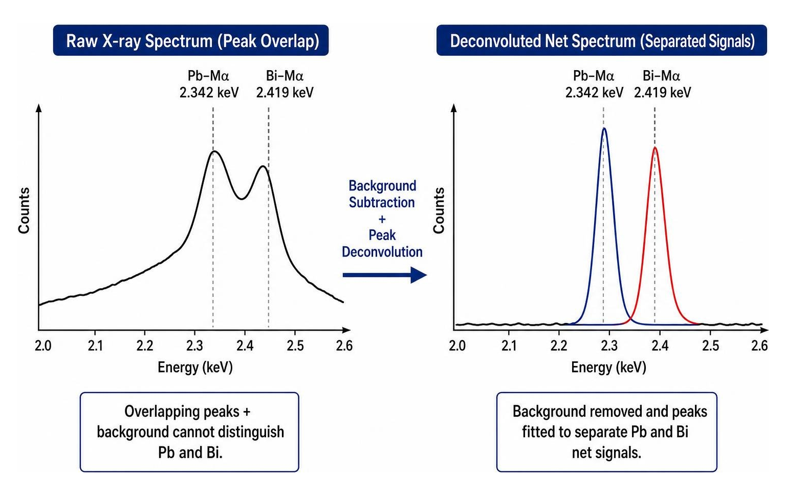
A classic example occurs in solder alloys containing lead (Pb) and bismuth (Bi). The Pb-$M\alpha$ peak (2.342 keV) and the Bi-$M\alpha$ peak (2.419 keV) overlap heavily in standard EDS detectors. A count map cannot tell these elements apart, resulting in identical, blurred maps. A net map uses peak fitting profiles derived from standard reference spectra to separate the signal into true lead and bismuth distributions. For further reading on EDS processing, explore EDS Elemental Mapping Principles.
Quantitative Concentration Mapping and Matrix Corrections
To convert X-ray counts into true elemental weight percentages, quantitative maps apply rigorous physics-based matrix corrections, such as ZAF or $\phi(\rho z)$ methods:
- Z (Atomic Number Effect): Adjusts for electron backscattering and stopping power variations.
- A (Absorption Effect): Corrects for X-rays absorbed by other elements inside the sample before reaching the detector.
- F (Fluorescence Effect): Accounts for secondary X-rays generated when characteristic emissions excite neighboring atoms.
Without matrix corrections, raw maps can be dangerously misleading. For instance, in mineral specimens where calcium occurs in both oxide and carbonate phases, ignoring matrix absorption can introduce quantitative errors of up to 60%. Advanced approaches to solving these complex matrix effects are detailed in Mineral Phase-Resolved Quantification in LA-ICP-MS Imaging.
Desktop SEM Software Features and Execution Parameters
Modern desktop Scanning Electron Microscope (SEM) software has transformed elemental mapping analysis into an intuitive, real-time workflow. Analysts no longer need to wait hours after acquisition to view spatial distributions.
Pixel Resolution and Dwell Time Configuration
Configuring an elemental map involves balancing spatial resolution, signal sensitivity, and total acquisition time. Key software parameters include:
- Pixel Resolution: Ranges from quick $32 \times 32$ pixel screening grids up to crisp $960 \times 960$ pixel maps.
- Pixel Dwell Time: Selectable from 1 to 500 milliseconds per pixel.
- Pass Accumulation: Summing multiple rapid sweeps reduces thermal drift and sample charging while building signal-to-noise ratio over time.
For fine microstructural features, longer dwell times or multiple pass sweeps allow high-count spectral accumulation per pixel without overloading the detector.
Line Scan Vector Analysis Along Sample Cross-Sections
When evaluating linear features—such as diffusion couples, multilayer coatings, or weld interfaces—a 2D map can sometimes provide more data than necessary. Software line scans allow operators to draw up to 12 linear vectors directly across a microstructural feature.

Line scan routines operate at resolutions between 16 and 512 points per line, with point dwell times typically set between 50 and 250 milliseconds. The resulting output displays element intensity or concentration profiles along a clear 1D position graph.
Real-Time Peak Deconvolution Without Pixel Binning
Historically, mapping software relied on pixel binning—combining adjacent pixels together—to gather enough X-ray counts for peak fitting. However, binning significantly reduces the true spatial resolution of the microscope.
Advanced live mapping software solves this issue by deconvoluting overlapping spectral signals in real time while maintaining individual pixel data. Every single pixel retains its full spectral dataset. Analysts can toggle specific element channels on or off during live acquisition or long after testing is complete without needing to re-scan the sample.
Cryo-EM Macromolecular Mapping with REEL Analysis
While SEM and EDS excel at inorganic materials, biological macromolecular complexes present unique challenges. Strikingly, an estimated one-third to one-half of all metalloprotein structures deposited in the Protein Data Bank (PDB) contain errors in metal ion assignments. Because single-particle analysis (SPA) cryo-EM generated one-third of all newly deposited structures in the PDB in 2023, correcting these spatial element assignments is vital for modern biochemistry.
Overcoming Radiation Damage in Biological Cryo-EM
Biological specimens are extremely sensitive to radiation damage. Standard high-resolution biological cryo-EM restricts total electron doses to a strict window of 30 to 60 $e^-/\text{\AA}^2$. Exceeding this limit breaks chemical bonds and degrades structural integrity.
However, detecting a single metal atom in a biological matrix using Electron Energy-Loss Spectroscopy (EELS) theoretically requires an electron dose of at least $10^7 e^-/\text{\AA}^2$—a threshold more than five orders of magnitude higher than the sample can survive without being destroyed.
Implementation Steps for Cryo-EM Elemental Mapping Analysis
To bridge this gap, researchers developed Reconstructed Electron Energy-Loss (REEL) analysis. REEL achieves high total electron doses without destroying individual biological complexes by spreading the dose across thousands of identical particle copies in 3D space.
The step-by-step methodology for REEL analysis includes:
- Low-Dose STEM-EELS Acquisition: Collect spectral image stacks in STEM mode using total doses below 100 $e^-/\text{\AA}^2$.
- Pose Estimation via Elastic Bright-Field (EBF) Images: Derive particle orientation poses from zero-loss EBF reference images rather than weak energy-loss signals.
- Unnormalized Reconstruction in RELION: Modify processing software routines (such as RELION) to eliminate origin normalization, preserving linear intensity scales across energy loss bins.
- Fourier Volume Padding: Apply 8-fold zero padding during reconstruction to eliminate corner intensity artifacts.
- 3D Spectral Averaging: Accumulate energy loss signals across thousands of aligned particles (e.g., 460,651 particles for ryanodine receptor RyR1).
This process achieves an effective accumulated electron dose of approximately $1.7 \times 10^8 e^-/\text{\AA}^2$, exceeding single-atom sensitivity thresholds while yielding 3D elemental maps, such as achieving a 40 $\text{\AA}$ spatial resolution at the carbon ionization edge. Facilities offering advanced electron microscopy systems are detailed at Transmission Electron Microscope Facilities.
Detectable Core-Loss Elements and Detection Thresholds
REEL analysis targets characteristic core-loss ionization edges to identify essential biological components:
- Carbon Edge (~284 eV): Differentiates protein frameworks and lipid micelles from surrounding aqueous solvent.
- Nitrogen (~401 eV) & Oxygen (~532 eV) Edges: Profile backbone structures, nucleic acids, and hydration shells.
- Buffer Ions & Bound Metal Cofactors: Pinpoint bound iron, calcium, magnesium, or zinc atoms within catalytic active sites.
Advanced Laser and Plasma Mapping Techniques
Beyond electron beams, advanced laser- and plasma-based mapping methods offer exceptional trace element sensitivity and rapid spatial profiling across large surface areas. For an in-depth explanation of laser micro-analysis, read What is Laser Ablation ICP-MS and How Does It Work?.
High-Speed Mapping via LIBS and LA-ICP-MS
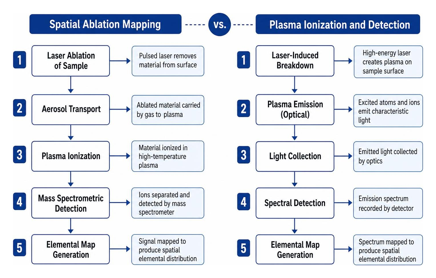
Two prominent technologies for high-speed spatial imaging are Laser-Induced Breakdown Spectroscopy (LIBS) and Laser Ablation Inductively Coupled Plasma Mass Spectrometry (LA-ICP-MS).
- Laser-Induced Breakdown Spectroscopy (LIBS): Uses high-energy laser pulses to form a localized plasma on the sample surface. LIBS operates at ambient pressure, requires no aerosol transport line, achieves kHz pulse acquisition rates, and seamlessly maps light non-metals like hydrogen, carbon, nitrogen, and oxygen.
- LA-ICP-MS Mapping: Ablates micro-scale particles and transports the aerosol to an ICP torch for mass analysis. While subject to minor wash-out delays in aerosol transport lines, modern time-of-flight systems enable multi-element trace spatial mapping down to parts-per-million detection levels.
To calibrate complex multi-phase maps acquired via laser ablation, researchers utilize post-processing workflows such as the XMapTools data reduction protocol. Comprehensive reviews of laser optical mapping setups are further detailed in the Review of elemental mapping by LIBS.
Frequently Asked Questions About Elemental Mapping
What is elemental mapping and what does it reveal about a sample?
Elemental mapping is an analytical technique that measures element-specific signals point-by-point across a sample area to generate color-coded 2D or 3D chemical images. It reveals the exact spatial distribution of chemical elements, highlighting microstructural zonation, localized contaminants, coating interfaces, and phase boundaries that bulk chemical testing cannot detect.
How does net mapping improve accuracy over raw count maps?
Net mapping removes background radiation (Bremsstrahlung) and applies spectrum deconvolution to separate overlapping characteristic energy peaks (such as lead and bismuth emissions). In contrast, raw count maps record all energy detected inside a fixed window, which often introduces signal distortion in areas with high background noise or overlapping elements.
What future developments will enhance elemental mapping resolution and sensitivity?
Future enhancements in elemental mapping center on ultra-fast direct electron detectors, integrated machine learning algorithms for automatic phase segmentation, and hybrid STEM-EELS systems. These developments will enable sub-nanometer spatial resolution, faster scan speeds, and improved sensitivity for light elements and trace cofactors in delicate biological and semiconductor samples.
Conclusion

From failure analysis in advanced manufacturing to resolving cofactor placement in structural biology, elemental mapping analysis transforms abstract chemical numbers into intuitive spatial insights. By choosing the right mapping approach—whether count, net, or fully quantitative maps—analysts can solve complex material challenges with confidence.
At Elemental Analysis Inc., we specialize in advanced trace element identification, quantification, and spatial characterization. Operating as a premier analytical facility, we provide high-precision testing solutions—including non-destructive Particle Induced X-ray Emission (PIXE)—with fast turnaround times and competitive pricing.
Ready to unlock the spatial secrets hidden within your materials? Explore our full range of analytical testing services at Discover Analytical Testing Services.